Sometimes, for the sake of economy and reduced weight the first filter choke is omitted from a valve amplifier power supply and replaced by a resistor. The resulting RC filter provides enough smoothing for push-pull amplifiers which naturally have high power supply rejection but is often inadequate for single ended amplifiers, leading to excessive 100 or 120 Hz hum.
The proposed circuit replaces the filter resistor and provides an output impedance, as seen by the filter capacitor, which closely resembles an inductor or choke in series with a smaller resistor.
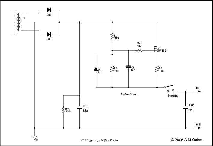
The circuit shown in the diagram above represents a power supply for a typical valve amplifier in which the usual filter choke has been replaced by an 'active choke' incorporating a high voltage FET.
In choosing the values for the components it is necessary to start with a target voltage drop and current in the quiescent state. Sufficient volts must appear across the FET to accommodate the ripple voltage on the reservoir capacitor while maintaining the FET fully saturated. On the other hand, excessive voltage will lead to unnecessary power dissipation in the FET. R3 is chosen to drop enough volts to swamp any variations in the turn on voltage of the FET. The potential divider ratio R1/R2 is chosen to provide the correct bias voltage for the FET, assuming the given overall voltage and current. C1 with R1 and R2 provides the time constant that gives the inductive output impedance. D1, which is normally off, limits the gate drive and hence the maximum output current. R4 is a 'gate stopper' that prevents high frequency instability. In normal operation, the voltage across the FET is small. The worst case occurs when the amplifier is turned on from standby.
An analysis of the dynamic behaviour and equivalent circuit of the circuit is given below.
Active Inductor Output Impedance
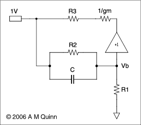
Consider the equivalent circuit in the above diagram.
The input terminal with one volt applied represents the output terminal at which we wish to determine the source impedance. The unity gain buffer and the 1/gm resistor represent the FET. The outer end of R1, being connected to the large reservoir capacitor, is effectively at zero for alternating signals.
In what follows, resistance and admittance will be interchanged where convenient, Yx = 1/Rx. Initially, 1/gm will be set to zero.
The voltage Vb is given by Millman's theorem:
Vb=(Y2+jωC)/(Y1+Y2+jωC)
This is passed through the buffer to the end of R3 so the voltage across R3 will be:
Vr3 = 1 - (Y2+jωC)/(Y1+Y2+jωC)
Expanding
Vr3 = ((Y1+Y2+jωC) - (Y2+jωC))/(Y1+Y2+jωC)
Vr3 = Y1/(Y1+Y2+jωC)
Thus the current taken via R3 is
Y3 * Vr3 = Y1*Y3/(Y1+Y2+jωC)
Therefore the effective admittance at the input terminal due to Y3 is
Yin = Y1*Y3/(Y1+Y2+jωC)
The impedance at the input terminal is 1/Yin
Zin = (Y1+Y2+jωC)/(Y1*Y3)
Zin = R3*(1+R1/R2) + jωC*R1*R3
This is equivalent to a resistor R3*(1+R1/R2) in series with an inductor C*R1*R3
The actual value of 1/gm is not zero, but it can simply be added to R3.
In addition, C1 effectively bypasses R2 so that R1 appears in parallel with the equivalent series LR combination at high frequencies. This is not a problem in practice.
© 2006 Arthur M Quinn

This work is licensed under a Creative Commons Attribution 2.0 UK: England
& Wales License.