This paper describes a further development and simplification of the emulation of a triode amplifier stage of the type typically found in a guitar amplifier. The emulation includes predominantly second order non-linearity at low levels, transitioning to mainly third order as the level increases together with clipping at the input due to grid current and clipping at the output due to cutoff. The main non linear element is a bipolar transistor and the input clipping level is approximately temperature compensated on the assumption that the stage will have to operate over an ambient temperature range of 0C to 30C.
Why Use A BJT? - The Problem With JFETs
The reasons for preferring BJTs to the more superficially valve-like FETs are given in the previous paper.
Transfer function
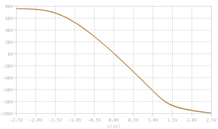
The transfer function of an amplifier is a plot of the output voltage against input voltage. The overall transfer function of a common cathode triode stage can be envisaged as being in three parts.
- A central section, almost linear with second order and much smaller third order components.
- A fairly rapid soft clipping above a threshold for positive inputs.
- A slower soft clipping towards cutoff for negative inputs.
These three sections blend together seamlessly as shown below.
In addition, the input resistance of the triode falls rapidly when the grid voltage is brought above that of the cathode and the grid current rises.
Schematic: Non-Linear Gain Stage for Internal Use
The schematic below shows a complete gain stage adapted for use within an amplifier. The input clipping level is about half that of an ECC83 stage and the expected range of source and load impedances is lower. In contrast with the previous example, no extra circuitry has been included to explicitly model cutoff at large negative inputs. Instead, a higher degree of feedback is used than in the original paper. This marginally increases the amount of third harmonic but still leaves the low level distortion predominantly second harmonic. It also increases the maximum drive level that can be applied to Q1, assisting in adjusting the internal parameters to reduce the noise, and sharpens the transition to cutoff, effectively removing the need for the cascode arrangement of the original paper. The overall gain is 17.3dB.
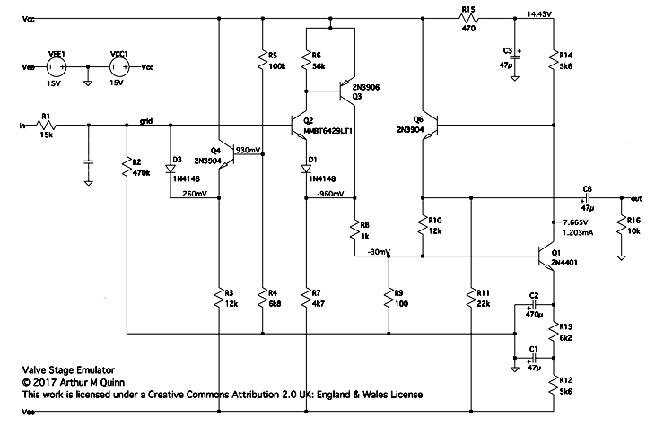
The main gain and non-linear transistor is Q1 which is biased to about 1.2mA via R12 and R13. The emitter of Q1 is decoupled to ground by C2, which has to have such a high value to decouple the low effective emitter resistance of about 60Ω. This is the 23Ω emitter resistance of Q1 modified by feedback. The output is developed across R14 and is buffered by emitter follower Q6 which also drives the feedback resistor R10.
The input diode D3, representing the grid - cathode diode, is biased by a separate potential divider R5/R4 which is buffered by Q4 to provide approximate temperature compensation.
The input to Q1 is developed across R9 which is chosen to be of a low value to minimise noise. Feedback is via R6, buffered by Q6.
In order to provide a high input impedance, Q2 and Q3 form a unity gain input buffer which drives the summing point via R8. Positive inputs are limited by the D3 clipper. For negative inputs, D1 protects the base-emitter junction of Q2, allowing the base to be driven negative while preserving a high input impedance. The allowable negative input level is set by the maximum collector-base voltage of Q1 and exceeds the supply voltage. For large negative inputs, the buffer clips as the pulldown current through R7 becomes insufficient. This is arranged to take place after Q1 is cut off.
C3 with R15 provides decoupling of noise on the positive power rail while C1 with R12 similarly filters the negative supply.
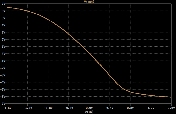
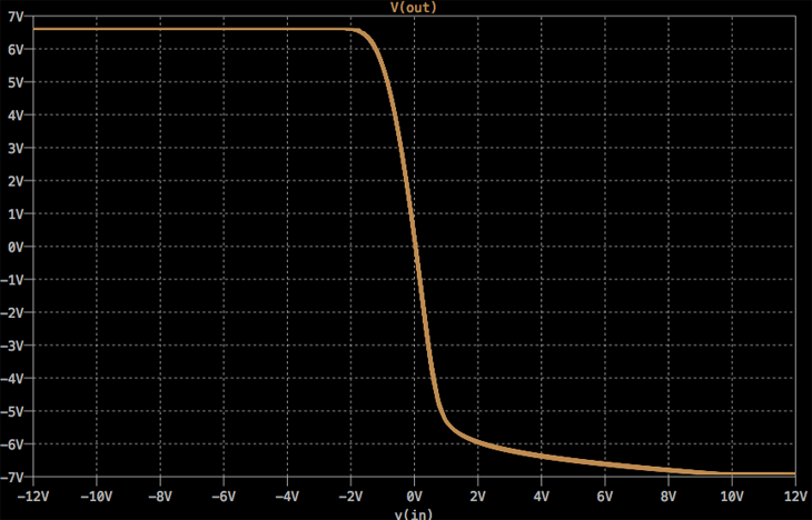
Transfer Function - Heavy Clipping
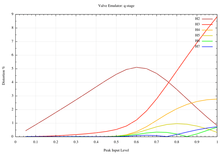
Harmonic Distortion VS Input Level
Noise
A major difficulty when attenuating the signal to the ~20mV required to drive Q1 is achieving adequate noise performance. Q1 is a medium power transistor known for its low extrinsic base resistance and hence good noise performance at low impedance levels. The source resistance for Q1 is kept low at 90Ω. Ideally, it would be lower than the the emitter resistance of 23Ω, but that would require considerably more power gain from the buffer and feedback network for very little improvement. Q2 is a "low noise" type, having a very high hfe at low currents. It is run at a collector current of ~20µA. The noise contributions of the other transistors are negligible and any general purpose type of reasonable gain will do. The CCIR-2K noise at the output is 28µ6V, corresponding to 3µ9V at the input. The CCIR-2K signal to noise ratio would be over 77dB for a 30mV input. As can be seen from the above graph, input clipping occurs at about 550mV peak or 389mV rms, at which point the signal to noise ratio would be 100 dB.
Miller Capacitance
The circuit as drawn does not include any capacitance between anode and grid. Instead, a capacitor can be included after R1 as shown unmarked to provide some high frequency filtering. If desired, a capacitor can be connected between the anode and the input. In order to achieve the same effect as the 2pF Cag of an ECC83, say, it would have to be roughly ten times larger to account for the lower overall gain. This capacitance, when viewed from the grid, would appear to be non-linear. Whether this is an effect worth reproducing is unknown.
© 2017 Arthur M Quinn

This work is licensed under a Creative Commons Attribution 2.0 UK: England
& Wales License.