Sometimes it will not be necessary to emulate every aspect of the triode stage behaviour. For example, it may not be necessary to model the grid current or the output impedance variations because of the way the stage is driven. In these circumstances it may be sufficient to model only the overall transfer function. A much simpler circuit is then possible. The following example assumes that the stage will have to operate over an ambient temperature range of 0C to 36C. This is no problem for the real valve, but requires temperature compenastion in the case of the bipolar emulator.
Schematic: Simplified Non-Linear Gain Stage for Internal Use
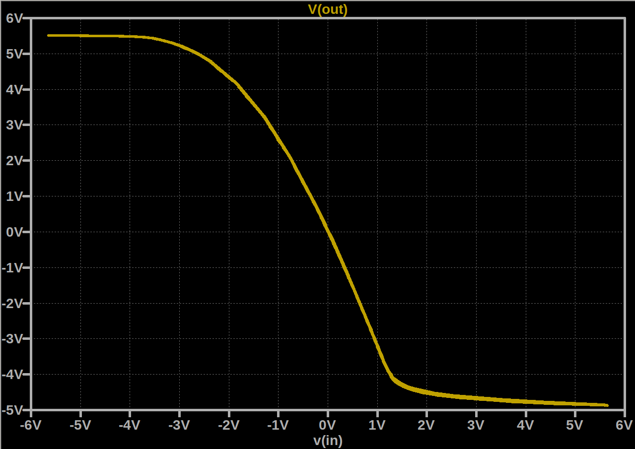
The schematic below shows a simplified gain stage adapted for use within an amplifier. A simple temperature compensated asymmetrical clipper drives a common emitter stage with local feedback produced by a resistor in the emitter circuit. The common emitter stage provides a rising second harmonic distortion that gradually changes to third harmonic at the clipping point.
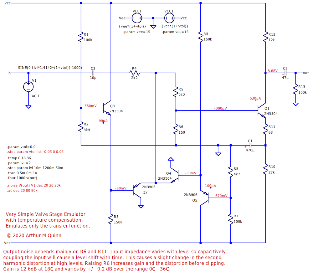
The main gain and non-linear transistor is Q1 which is biased to about 530µA via R10 and R11. The emitter of Q1 is decoupled to ground by C1. R11 provides local feedback.
Clipping of the input is carried out by Q2 and Q4 emitter base junctions. The temperature variation of the junction forward voltages is compensated by feeding the bases from Q3 and Q5 which provide complementary temperature variability.
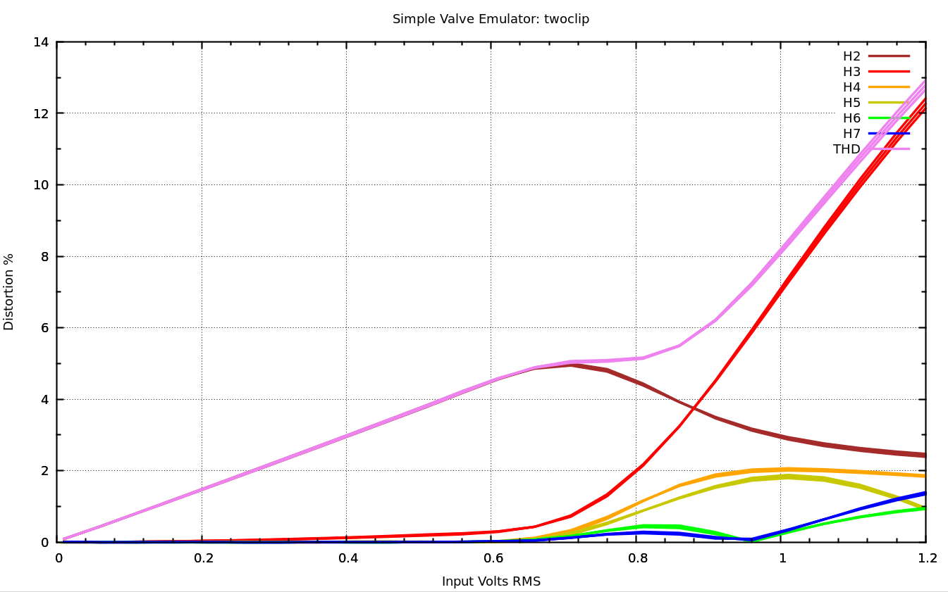
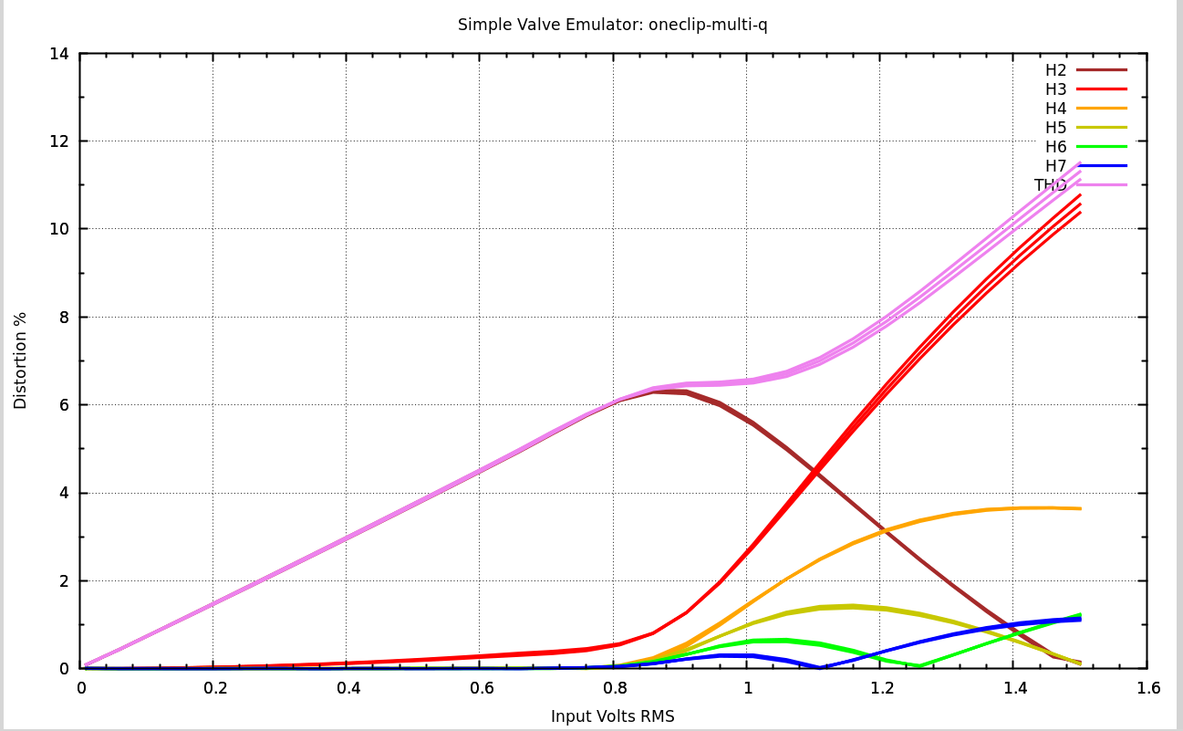
The distortion graph shows superimposed curves for the separate harmonics and the total distortion at three temperatures; 0C 18C and 36C. The three sets of curves are almost identical.
Harmonic Distortion VS Input Level
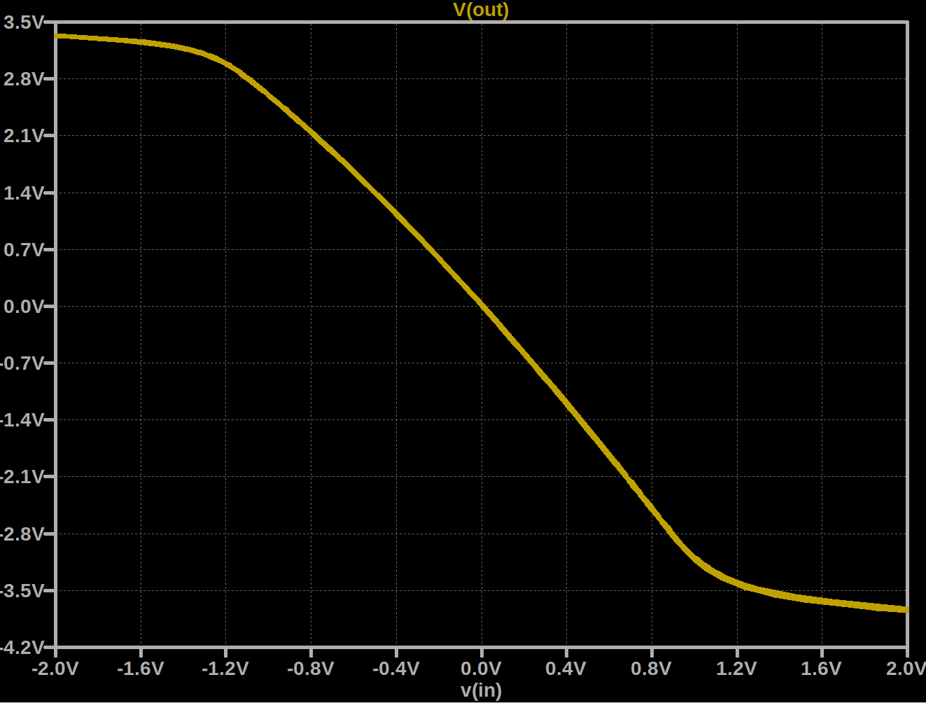
Gain and Noise
Output noise depends mainly on R6 and R11. Input impedance varies with level so capacitively coupling the input will cause a level shift with time. This causes a slight change in the second harmonic distortion at high levels. Raising R6 increases gain and the distortion before clipping. Gain is 12.6dB at 18C and varies by +/- 0.2 dB over the range 0C - 36C.
Schematic: Further Simplified Non-Linear Gain Stage for Internal Use - Single Clipper.
The schematic below shows a simplified gain stage adapted for use within an amplifier. A simple temperature compensated asymmetrical clipper drives a common emitter stage with local feedback produced by a resistor in the emitter circuit. The common emitter stage provides a rising second harmonic distortion that gradually changes to third harmonic at the clipping point.
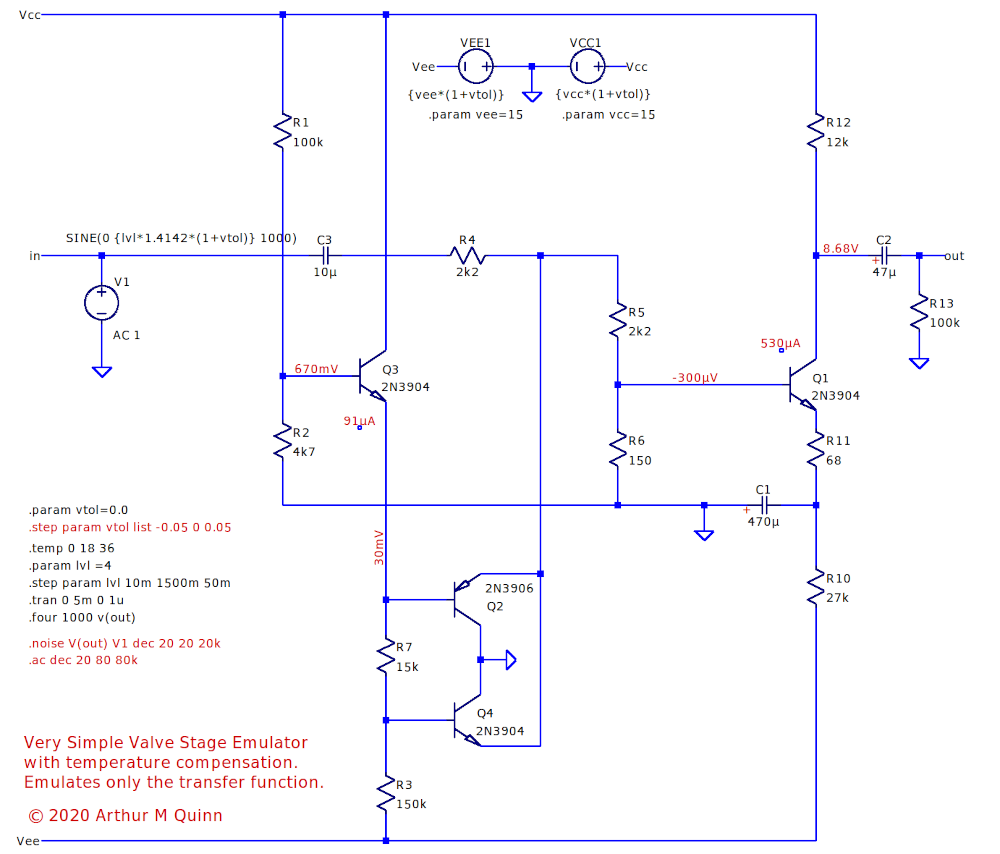
The main gain and non-linear transistor is Q1 which is biased to about 530µA via R10 and R11. The emitter of Q1 is decoupled to ground by C1. R11 provides local feedback.
Clipping of the input is carried out by Q2 emitter base junction. The temperature variation of the junction forward voltage of Q2 is compensated by feeding the base from Q3 which provides complementary temperature variability. Q4's base emitter forward voltage is not temperature compensated since it is biased to clip after Q1 is essentially turned off. Its purpose is to protect the base-emitter junction of Q2.
The distortion graph shows superimposed curves for the separate harmonics and the total distortion at three temperatures; 0C 18C and 36C. The three sets of curves are almost identical.
Harmonic Distortion VS Input Level
© 2020 Arthur M Quinn

This work is licensed under a Creative
Commons Attribution 2.0 UK: England & Wales
License.